Jun 4, 2026
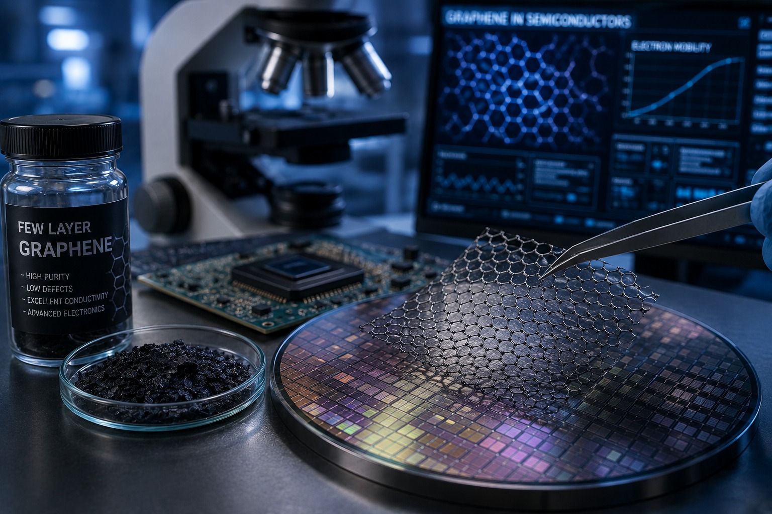
The contemporary landscape of solid-state physics is witnessing a seismic shift as graphene in semiconductors emerges as a transformative force within the global microelectronics supply chain. While silicon has long served as the fundamental bedrock of integrated circuits, its physical limitations are becoming increasingly apparent under the relentless pressure of Moore's Law. This two-dimensional honeycomb lattice of carbon atoms offers a spectacular departure from traditional material constraints, providing a platform where ballistic electron transport and exceptional thermal conductivity converge. For industrial stakeholders and enterprise-level innovators, integrating graphene in semiconductors represents not merely an incremental upgrade but a radical departure toward hyper-efficient electronic architectures.
How Graphene Can Support Advanced Electronics
The integration of graphene into the semiconductor ecosystem addresses the critical bottlenecks of power density and switching speeds. As we transition into the era of 2nm process nodes, the industry requires materials that maintain structural integrity while facilitating rapid electron mobility. Graphene in semiconductors provides the requisite physical properties to bypass the scattering effects typically found in metal-oxide interfaces. By leveraging these atomic-scale advantages, we can engineer devices that operate at terahertz frequencies, far surpassing the current benchmarks of commercial silicon-based logic gates.
Conductive Layers and Components
In the realm of high-frequency applications, the implementation of graphene as a conductive interfacial layer minimizes contact resistance, which is a primary hurdle in miniaturization. We observe that utilizing graphene in semiconductors allows for the development of transparent electrodes and ultra-thin interconnects that do not suffer from electromigration in the same way copper does. These components are essential for the next generation of optoelectronics and flexible logic boards where traditional brittle materials fail to meet the mechanical and electrical demands of industrial-grade hardware.
Heat Management in Electronic Devices
Thermal throttling remains the most persistent adversary of high-performance computing. However, the intrinsic lattice vibrations of carbon atoms enable heat dissipation rates that are fundamentally superior to any existing dielectric or metallic heat sink. When we incorporate graphene in semiconductors, the lateral heat spreading capability ensures that localized hot spots are neutralized before they can cause structural degradation of the chip. This allows for higher clock speeds and denser packing of transistors without the catastrophic risk of thermal runaway.
Material Testing for Future Chip Development
Transitioning from theoretical modeling to industrial-scale production requires rigorous material characterization and empirical validation. Our approach focuses on stress-testing these carbon-based layers under extreme fluctuating voltages and varying environmental conditions. By analyzing the synergistic relationship between graphene in semiconductors and traditional substrates like Gallium Nitride or Silicon Carbide, we pave the way for hybrid systems that combine the reliability of established platforms with the unprecedented performance of graphene.
Using Few Layer Graphene for Electronics Development
For organizations operating within the professional technology sector, the transition to graphene-enhanced systems often begins with Few Layer Graphene (FLG). This specific material morphology offers a pragmatic balance between the exotic properties of a single atomic sheet and the structural robustness required for standard industrial deposition processes.
Choose the Right Graphene Material Form
Selecting the appropriate medium, whether it be powders, dispersions, or films, is a critical decision for your research and development pipeline. For semiconductor integration, chemical vapor deposition films or high-purity FLG flakes are often preferred to ensure uniform coverage across the wafer. Making the correct choice at the inception of the design phase prevents costly recalibrations during the later stages of hardware prototyping.
Check the Material Specification
Precision is the hallmark of professional electronics manufacturing. You must scrutinize the lateral flake size, the number of layers, and the defect density, often measured via Raman spectroscopy. Minor variances in oxygen content or metallic impurities can significantly alter the doping profile of your semiconductor device. We emphasize the necessity of obtaining materials with documented consistency to ensure that your industrial output meets the stringent requirements of high-reliability aerospace or telecommunications equipment.
Source Graphene Materials for Industrial Research and Development
Navigating the global supply chain for advanced nanomaterials requires a partner that understands the nuances of enterprise-level logistics and quality control. Collaborative efforts between material scientists and electronics engineers are vital to move beyond laboratory curiosities. By sourcing high-grade materials, you empower your engineering teams to develop patentable intellectual property that will define the future of the digital economy. The evolution of the electronics industry is inextricably linked to our ability to harness the power of carbon at the molecular level. As we have explored, the strategic adoption of graphene-based solutions is the key to unlocking the next frontier of processing power and energy efficiency. To support your ventures in this high-stakes arena, Ravphene Ravelware stands as a premier producer of high-specification Few Layers Graphene. We provide the essential building blocks for your industrial innovations, ensuring that your transition into advanced semiconductor technology is backed by material excellence and technical expertise.
Recent Post

Extending Industrial Asset Lifespan Through Advanced Material Innovation
Aug 3, 2026

Building More Durable Infrastructure with Advanced Materials
Jul 28, 2026

Graphene in Smart Manufacturing: Enabling the Next Industrial Revolution
Jul 27, 2026
How Graphene Improves Corrosion Protection in Industrial Applications | RAVphene
Jul 21, 2026